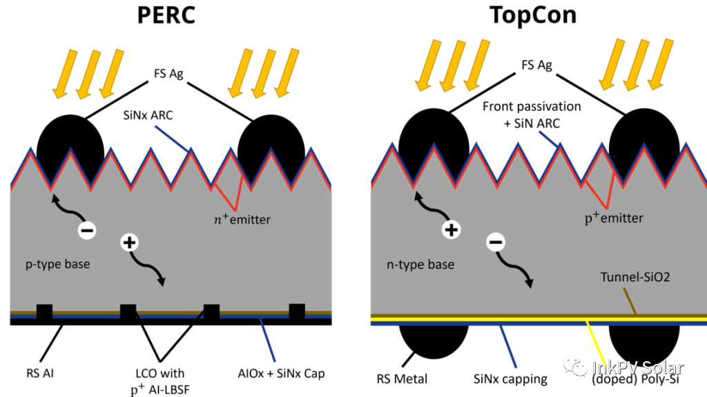
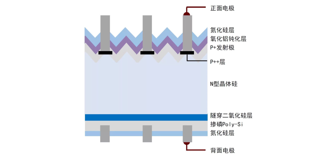
Main processes and their functions in TOPCon solar cell production
Wet Etching
① Purpose
After silicon wafers are cut, the edges may be damaged, and the crystalline structure of silicon is disrupted, leading to severe surface recombination. The main purpose of wet etching is to remove the surface damage and form a surface pyramid texture to trap light. When light shines on the silicon surface, it undergoes multiple refractions, reducing the reflectivity.
Boron Diffusion Process
① Purpose
The main purpose is to create a PN junction. As boron has a low solid solubility in silicon, high temperature and longer diffusion time are required. The choice of the diffusion source also affects the production process; chloride sources are highly corrosive, and bromide sources have high viscosity, making the cleaning process cumbersome and increasing maintenance costs.
Boron diffusion is a process used in semiconductor manufacturing to introduce boron atoms into a silicon substrate, creating a P-type doping layer. The process typically takes place at higher temperatures, exceeding 1000°C. Compared to the 102-minute cycle period required for phosphorus diffusion, the cycle time for boron diffusion is 150 minutes.
The principle behind boron diffusion involves placing the silicon wafers in a high-temperature furnace with a boron source, such as boron oxide (B2O3) or boron nitride (BN). At the elevated temperatures, boron atoms diffuse into the silicon lattice, replacing some of the silicon atoms and creating a P-type region. The depth of the boron diffusion can be controlled by adjusting the time and temperature parameters.
Boron-diffused regions create PN junctions when combined with N-type regions in silicon. These PN junctions are the basis for creating diodes and transistors, forming the foundation for various electronic devices used in modern technology.
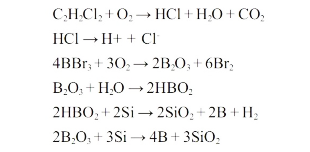
During the reaction in the furnace tube, gaseous HCl and H2O are uniformly distributed inside the tube, carried by N2. H2O also reacts with BBr3 and O2, generating gaseous HBO2 and B2O3. HBO2 further decomposes into B2O3 at high temperatures, facilitating the even distribution of B2O3 on the surface of the solar cell.
Moreover, H2O reacts with the deposited B2O3 inside the furnace tube, preventing the deposition of B2O3 on the diffusion tube walls. This extends the lifespan of the quartz devices and increases the effective boron source.
HCl can also react with metal impurities on the surface of the solar cell and inside the furnace tube, forming gaseous metal chlorides that are carried away in the exhaust gas. This process prevents metal impurities from diffusing into the interior of the solar cell during high-temperature procedures.
SE Laser Doping Process
① Purpose
The main purpose of the SE (Selective Emitter) laser doping process is to create a selective emitter region in a solar cell. This process involves high-concentration doping in the area where the metal grid lines make contact with the silicon wafer and its vicinity, reducing the contact resistance between the front metal electrode and the silicon. Meanwhile, low-concentration doping is performed in regions outside the electrode area to lower the recombination in the diffusion layer.
By optimizing the emitter region, the SE laser doping process increases the output current and voltage of the solar cell, thereby enhancing the photovoltaic conversion efficiency.
② The SE Laser Doping process in TOPCon:
In the TOPCon process, the SE (Selective Emitter) laser doping step takes place after the deposition of the tunnel oxide layer and the intrinsic polycrystalline silicon passivation layer. During this step, the laser is used to selectively introduce boron into the silicon wafer, creating a selective emitter region with high-concentration boron doping in the contact areas and low-concentration boron doping in the non-contact areas.
Compared to the traditional boron diffusion process, introducing boron into silicon using SE laser doping is more challenging. Boron and phosphorus have different separation coefficients, with phosphorus diffusing more easily from silicon dioxide to silicon compared to boron. As a result, higher energy is required to drive the boron doping, and excessive laser energy can lead to silicon wafer damage. This difficulty in boron doping is one of the challenges in implementing the SE laser doping process in the TOPCon cell technology.
Nevertheless, by employing SE laser doping, TOPCon cells can theoretically achieve an efficiency improvement of 0.5%, and in practical mass production, an efficiency gain of 0.2 to 0.4% is attainable compared to traditional boron diffusion methods.
Etching Process
① Purpose
The main purpose of the etching process is to remove Back Surface Field (BSF) and the back junction of the solar cell. During the diffusion process, a diffusion layer is formed on the surface and surrounding areas of the silicon wafer. The diffusion layer around the edges is prone to short-circuiting, and the surface diffusion layer can interfere with subsequent passivation steps. Therefore, it needs to be removed.
Currently, the etching process is mainly carried out using a wet-etching method. The back surface and surrounding diffusion layers are first removed in a chain-type equipment, followed by processing the front surface of the solar cell.
Preparation of Tunnel Oxide Layer and Polycrystalline Silicon Layer
① Purpose
The main purpose is to deposit a 1-2 nm tunnel oxide layer on the backside of the solar cell, followed by the deposition of a 60-100 nm polycrystalline silicon layer to form a passivated contact structure. There are various methods to prepare the passivation layer in TOPCon technology, mainly including LPCVD (Low-Pressure Chemical Vapor Deposition), PECVD (Plasma-Enhanced Chemical Vapor Deposition), and PVD (Physical Vapor Deposition) routes. Currently, LPCVD is the dominant method, but it suffers from wrap-around issues. PECVD, on the other hand, shows strong potential due to its overall performance.
Front-Side Aluminum Oxide Deposition
① Purpose
The purpose is to deposit a layer of aluminum oxide film on the front side of the silicon wafer, which, together with other layers, contributes to front-side passivation.
Preparation of Front-Side Anti-Reflection Coating
① Purpose
The purpose of the front-side anti-reflection coating is similar to that of the backside. Additionally, the front-side aluminum oxide film is very thin and can be easily damaged during subsequent solar cell assembly. The front-side SiNx also provides protection for the aluminum oxide layer.
Screen Printing and Laser Transfer Printing
Currently, screen printing is commonly used in the solar cell printing process. However, in the context of reducing silver consumption in N-type cells, laser transfer printing technology (Pattern Transfer Printing) may have advantages.
Laser transfer printing is a new non-contact printing technology, where the desired paste is coated on a specific flexible transparent material. High-power laser beams are used to scan and transfer the paste from the flexible transparent material to the solar cell surface, forming grid lines and preparing front and rear electrodes.
Sintering
Sintering is carried out at high temperatures to form good ohmic contacts.
Automated Sorting
Automated sorting is used to classify solar cells based on their different conversion efficiencies.